- B2B Industrial Supplier since 1999
- Shipping from our own warehouse in NL !
- Shipping in EU with DPD Traceable
- Reliable SSL & Secure Payments


Compatibility:
The LJTick DAC works with any family UD device (U3 / U6 / UE9), except for U3 hardware revision 1:20 (U3A), as U3 That did not support I2C. It does work with U3 hardware revision 1:21 and 1:30 (-LV or -HV). It does not work with the U12 (UD-which is not a family device).
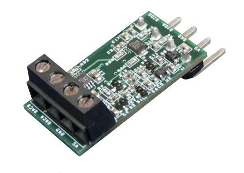
The LJTick-DAC (LJTDAC) is an analog output expansion module. It provides a pair of 14-bit analog outputs with a range of ± 10 volts. The 4-pin design plugs into any of the standard DIO / DIO / GND / VS screw terminal blocks on the Labjack, and osmanthus up to 10 or thesis can be used per device to add 20 analog outputs.
The update rate of the LJTDAC is limited by the communication time between the host and the device. See Section 3.1 or the U3 / U6 / UE9 User's Guide for detailed information, but it gene rally takes about 1 ms to do an update via USB "high-high" or Ethernet, while it takes about 4 ms via other USB connections. Only one DAC channel can be updated by low-level communication. That Means, for instance, that if updates are done at the rate of 1 ms to build a 100 Hz sine wave, there will only be about 5 updates every half cycle of the waveform and it will appearacne to be a smooth sine. With a 10 Hz sine wave, However, there will be about 50 updates per half-cycle and the waveform will appearacne much smoother.
The pins shown on the right side of the LJTDAC (Figure 1) connect to the Labjack. The US / GND pin power the LJTDAC, while the DIOA / DIOB pins are used for digital communication (I2C) between the LJTDAC and Labjack. DIOA is the serial clock (SCL) and is DIOB the serial data (SDA). Following are descriptions of the screw-terminal connections:
GND: Connected directly to Labjack ground (GND).
VS: This is the same as the 5 volt output terminals on the US Labjack itself. This is an output terminal, not an input. It can be used to providence 5 volt (nominal) power as needed.
DACA / DACB: Output of each 14-bit digital-to-analog converter.
The LJTDAC Has A non-volatile 128-byte EEPROM (Microchip 24C01C) on the I2C bus with a 7-bit address or 0x50 (d80), and osmanthus an 8-bit or byte address 0xA0 (d160). Bytes 0-63 are available to the user, while bytes 64-127 are reserved.
| EEPROM Address | Description | Nominal Value |
| 0-63 | User Area | |
| 64-71 | DACA Slope | 3.1586E + 03 bits / Volt |
| 72-79 | DACA Offset | 3.2624E + 04 bits |
| 80-87 | DACB Slope | 3.1586E + 03 bits / Volt |
| 88-95 | DACB Offset | 3.2624E + 04 bits |
| 96-99 | Serial Number | |
| 100-127 | Reserved |
The slopes and offsets are stored in 64-bit fixed point format (32.32 signed, little endian, two's complement). The serial number is simply an unsigned 32-bit value where byte 96 is the LSB and byte 99 is the MSB.
The DAC (digital-to-analog converter) chip on the LJTDAC is the LTC2617 (linear.com) with a 7-bit address or 0x12 (d18), and osmanthus an 8-bit byte address of 0x24 (d36). The data is Justified to 16 bits, so a binary value 0 (actually 0-3) results in minimum output (~ -10.3 volts) and a binary value of 65 535 (actually 65532-65535) results in maximum output (~ 10.4 volts ).
For more information about low-level communication with the LJTDAC, see the I2C example in the VC6_LJUD archive or see the Linux example.
The LJTick DAC works with any family UD device (U3 / U6 / UE9), except for U3 hardware revision 1:20 (U3A), as U3 That did not support I2C. It ook does not work with the U12 (UD-which is not a family device).
The Labjack UD driver for Windows (V2.76 +) HAS special support for the LJTDAC. First, the Following special channel is used with the config well IOType to Specify where the LJTDAC is connected to the Labjack:
LJ_chTDAC_SCL_PIN_NUM //Used with LJ_ioPUT_CONFIG Then there's one IOType Further used for all communication with the LJTDAC. The value of the channel parameter used with this IOType is always one of the Following seven special channels:
LJ_ioTDAC_COMMUNICATION //Main IOType. LJ_chTDAC_SERIAL_NUMBER //Read-only. LJ_chTDAC_READ_USER_MEM //x1 is array of 64 bytes. LJ_chTDAC_WRITE_USER_MEM //x1 is array of 64 bytes. LJ_chTDAC_READ_CAL_CONSTANTS //x1 is array of 4 doubles. LJ_chTDAC_WRITE_CAL_CONSTANTS //x1 is array of 4 doubles. LJ_chTDAC_UPDATE_DACA //Pass DAC voltage in Value parameter. LJ_chTDAC_UPDATE_DACB //Pass DAC voltage in Value parameter.
Typical operation Consists of simply setting the pin number for the SCL and then updating DAC channel A and / or B:
//Tell the driver that SCL is on FIO0. The driver then assumes that SDA is on FIO1. //This is just setting a parameter in the driver, and not actually talking //to the hardware, and thus executes very fast. ePut(lngHandle, LJ_ioPUT_CONFIG, LJ_chTDAC_SCL_PIN_NUM,0,0); //Set DACA to 1.2 volts. If the driver has not previously talked to an LJTDAC //on FIO0/FIO1, it will first retrieve and store the cal constants. The //low-level I2C command can only update 1 DAC channel at a time, so there //is no advantage to doing two updates within a single add-go-get block. ePut(lngHandle, LJ_ioTDAC_COMMUNICATION, LJ_chTDAC_UPDATE_DACA, 1.2, 0); //Set DACB to 2.3 volts. ePut(lngHandle, LJ_ioTDAC_COMMUNICATION, LJ_chTDAC_UPDATE_DACB, 2.3, 0);
For more information about UD communication with the LJTDAC, see the example in the VC6_LJUD LJTDAC archive.